- 您现在的位置:买卖IC网 > Sheet目录3878 > PIC18F4610T-I/ML (Microchip Technology)IC MCU FLASH 32KX16 44QFN
2009 Microchip Technology Inc.
DS39636D-page 101
PIC18F2X1X/4X1X
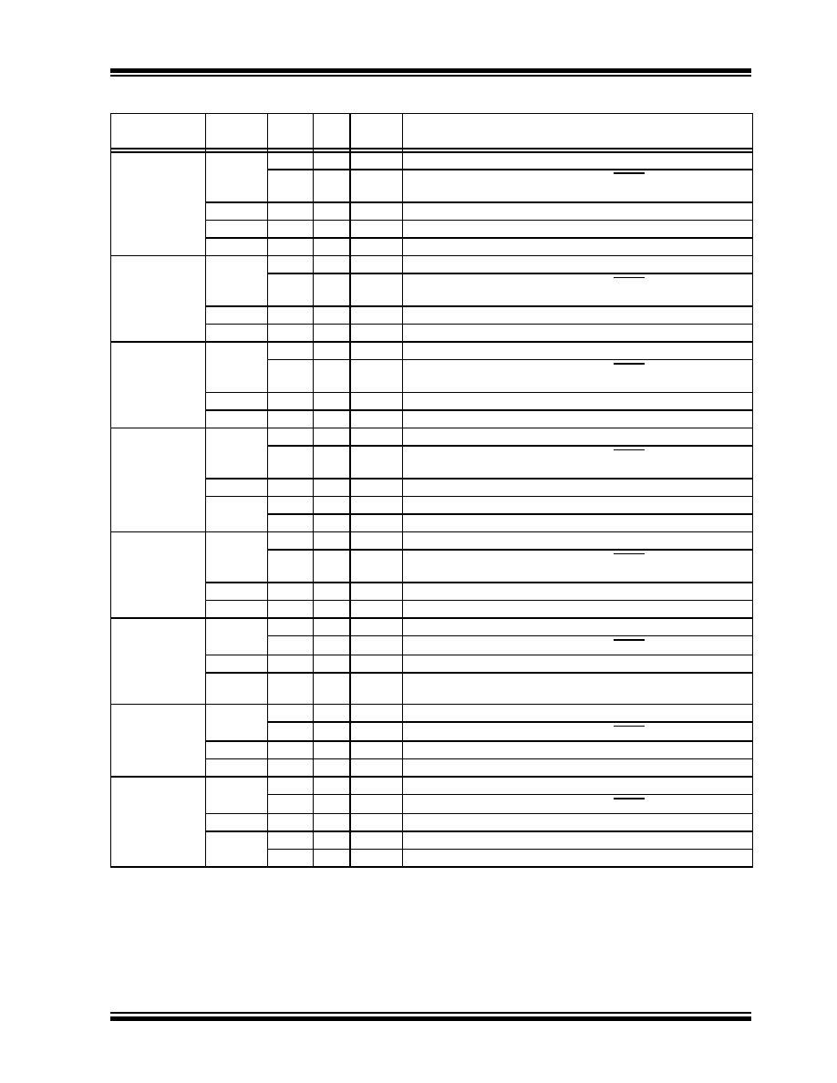
TABLE 9-3:
PORTB I/O SUMMARY
Pin
Function
TRIS
Setting
I/O
Type
Description
RB0/INT0/FLT0/
AN12
RB0
0
O
DIG
LATB<0> data output; not affected by analog input.
1
I
TTL
PORTB<0> data input; weak pull-up when RBPU bit is cleared.
Disabled when analog input enabled.(1)
INT0
1
I
ST
External interrupt 0 input.
FLT0
1
I
ST
Enhanced PWM Fault input (ECCP1 module); enabled in software.
AN12
1
I
ANA
A/D input channel 12.(1)
RB1/INT1/AN10
RB1
0
O
DIG
LATB<1> data output; not affected by analog input.
1
I
TTL
PORTB<1> data input; weak pull-up when RBPU bit is cleared.
Disabled when analog input enabled.(1)
INT1
1
I
ST
External interrupt 1 input.
AN10
1
I
ANA
A/D input channel 10.(1)
RB2/INT2/AN8
RB2
0
O
DIG
LATB<2> data output; not affected by analog input.
1
I
TTL
PORTB<2> data input; weak pull-up when RBPU bit is cleared.
Disabled when analog input enabled.(1)
INT2
1
I
ST
External interrupt 2 input.
AN8
1
I
ANA
A/D input channel 8.(1)
RB3/AN9/CCP2
RB3
0
O
DIG
LATB<3> data output; not affected by analog input.
1
I
TTL
PORTB<3> data input; weak pull-up when RBPU bit is cleared.
Disabled when analog input enabled.(1)
AN9
1
I
ANA
A/D input channel 9.(1)
CCP2(2)
0
O
DIG
CCP2 compare and PWM output.
1
I
ST
CCP2 capture input
RB4/KBI0/AN11
RB4
0
O
DIG
LATB<4> data output; not affected by analog input.
1
I
TTL
PORTB<4> data input; weak pull-up when RBPU bit is cleared.
Disabled when analog input enabled.(1)
KBI0
1
I
TTL
Interrupt on pin change.
AN11
1
I
ANA
A/D input channel 11.(1)
RB5/KBI1/PGM
RB5
0
O
DIG
LATB<5> data output.
1
I
TTL
PORTB<5> data input; weak pull-up when RBPU bit is cleared.
KBI1
1
I
TTL
Interrupt on pin change.
PGM
x
I
ST
Single-Supply Programming mode entry (ICSP). Enabled by LVP
Configuration bit; all other pin functions disabled.
RB6/KBI2/PGC
RB6
0
O
DIG
LATB<6> data output.
1
I
TTL
PORTB<6> data input; weak pull-up when RBPU bit is cleared.
KBI2
1
I
TTL
Interrupt on pin change.
PGC
x
I
ST
Serial execution (ICSP) clock input for ICSP and ICD operation.(3)
RB7/KBI3/PGD
RB7
0
O
DIG
LATB<7> data output.
1
I
TTL
PORTB<7> data input; weak pull-up when RBPU bit is cleared.
KBI3
1
I
TTL
Interrupt on pin change.
PGD
x
O
DIG
Serial execution data output for ICSP and ICD operation.(3)
x
I
ST
Serial execution data input for ICSP and ICD operation.(3)
Legend:
DIG = Digital level output; TTL = TTL input buffer; ST = Schmitt Trigger input buffer; ANA = Analog level input/output;
x = Don’t care (TRIS bit does not affect port direction or is overridden for this option).
Note 1:
Configuration on POR is determined by the PBADEN Configuration bit. Pins are configured as analog inputs by default
when PBADEN is set and digital inputs when PBADEN is cleared.
2:
Alternate assignment for CCP2 when the CCP2MX Configuration bit is ‘0’. Default assignment is RC1.
3:
All other pin functions are disabled when ICSP or ICD are enabled.
发布紧急采购,3分钟左右您将得到回复。
相关PDF资料
PIC18F4610-E/PT
IC MCU FLASH 32KX16 44TQFP
PIC18F4610-E/ML
IC MCU FLASH 32KX16 44QFN
PIC18LF2331T-I/SO
IC MCU FLASH 4KX16 28SOIC
PIC18F4515T-I/PT
IC MCU FLASH 24KX16 44TQFP
PIC18F4431T-I/ML
IC MCU FLASH 8KX16 44QFN
PIC18F4431-E/ML
IC MCU FLASH 8KX16 44QFN
PIC18F4410T-I/ML
IC MCU FLASH 8KX16 44QFN
PIC18F4410-E/PT
IC MCU FLASH 8KX16 44TQFP
相关代理商/技术参数
PIC18F4610T-I/PT
功能描述:8位微控制器 -MCU 64KB 3968 RAM 36 I/O RoHS:否 制造商:Silicon Labs 核心:8051 处理器系列:C8051F39x 数据总线宽度:8 bit 最大时钟频率:50 MHz 程序存储器大小:16 KB 数据 RAM 大小:1 KB 片上 ADC:Yes 工作电源电压:1.8 V to 3.6 V 工作温度范围:- 40 C to + 105 C 封装 / 箱体:QFN-20 安装风格:SMD/SMT
PIC18F4620-E/ML
功能描述:8位微控制器 -MCU 64KB 3968 RAM 36 I/O RoHS:否 制造商:Silicon Labs 核心:8051 处理器系列:C8051F39x 数据总线宽度:8 bit 最大时钟频率:50 MHz 程序存储器大小:16 KB 数据 RAM 大小:1 KB 片上 ADC:Yes 工作电源电压:1.8 V to 3.6 V 工作温度范围:- 40 C to + 105 C 封装 / 箱体:QFN-20 安装风格:SMD/SMT
PIC18F4620-E/P
功能描述:8位微控制器 -MCU 64KB 3968 RAM 36 I/O RoHS:否 制造商:Silicon Labs 核心:8051 处理器系列:C8051F39x 数据总线宽度:8 bit 最大时钟频率:50 MHz 程序存储器大小:16 KB 数据 RAM 大小:1 KB 片上 ADC:Yes 工作电源电压:1.8 V to 3.6 V 工作温度范围:- 40 C to + 105 C 封装 / 箱体:QFN-20 安装风格:SMD/SMT
PIC18F4620-E/PT
功能描述:8位微控制器 -MCU 64KB 3968 RAM 36 I/O RoHS:否 制造商:Silicon Labs 核心:8051 处理器系列:C8051F39x 数据总线宽度:8 bit 最大时钟频率:50 MHz 程序存储器大小:16 KB 数据 RAM 大小:1 KB 片上 ADC:Yes 工作电源电压:1.8 V to 3.6 V 工作温度范围:- 40 C to + 105 C 封装 / 箱体:QFN-20 安装风格:SMD/SMT
PIC18F4620-E/PT
制造商:Microchip Technology Inc 功能描述:IC 8BIT MCU PIC18F 40MHZ TQFP-44 制造商:Microchip Technology Inc 功能描述:IC, 8BIT MCU, PIC18F, 40MHZ, TQFP-44
PIC18F4620-I/ML
功能描述:8位微控制器 -MCU 64KB 3968 RAM 36 I/O RoHS:否 制造商:Silicon Labs 核心:8051 处理器系列:C8051F39x 数据总线宽度:8 bit 最大时钟频率:50 MHz 程序存储器大小:16 KB 数据 RAM 大小:1 KB 片上 ADC:Yes 工作电源电压:1.8 V to 3.6 V 工作温度范围:- 40 C to + 105 C 封装 / 箱体:QFN-20 安装风格:SMD/SMT
PIC18F4620-I/P
功能描述:8位微控制器 -MCU 64KB 3968 RAM 36 I/O RoHS:否 制造商:Silicon Labs 核心:8051 处理器系列:C8051F39x 数据总线宽度:8 bit 最大时钟频率:50 MHz 程序存储器大小:16 KB 数据 RAM 大小:1 KB 片上 ADC:Yes 工作电源电压:1.8 V to 3.6 V 工作温度范围:- 40 C to + 105 C 封装 / 箱体:QFN-20 安装风格:SMD/SMT
PIC18F4620-I/P
制造商:Microchip Technology Inc 功能描述:IC 8BIT FLASH MCU 18F4620 DIP40